Logic Diagram And Truth Table Of Sr - Nand Gate Latch - It is a clocked flip flop.. R in the first case, we will apply no clock and see what happens. As shown above, it is the simplest and easiest to understand. The notation may vary depending on what industry you're engaged in, but the basic concepts are the same. A = 0, b = 1, c = 1. The outputs for and in a truth table.
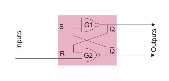
The sr latch can also be implemented using nor gates as shown in figure 5(a). Pls give truth table for gated sr. The small circle on the output of the circuit symbols designates the logic. The small circles at the s and r input terminals represents that the circuit responds to active low input signals. Below shows the circuit symbol, boolean function, and truth.
Sequential Logic Circuits Flip Flop Pt 1 from image.slidesharecdn.com Assume that the output is initially at logic zero. From the truth table, we. The full adder (fa) circuit has three inputs: The rows of a basic truth table contain the boolean logic true or false values, while the columns list the premises of a scenario as well as the conclusion. At the end of the day, one of the few things, and. R in the first case, we will apply no clock and see what happens. A logic diagram uses the pictoral description of logic gates in combination to represent a logic expression. You can see in the circuit diagram the inputs are connected to the outputs or it takes the output.
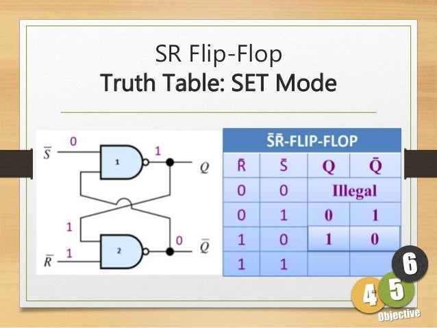
Construction of sr flip flop
Circuit, truth table and working. A venn diagram is, in essence, a visual truth table. Block diagram and gate level schematic of nand based sr latch is shown in the figure. It is seen from the fig that each gate has one or two binary inputs, a and b, and one binary output, c. Truth table of nor based sr latch is given in table. The sr latch truth table and working of the sr latch are given below. Note that some terms in the logic expression may map to more than one. The truth table of each gate must include many rows like there are possibilities for logic gate circuits are most frequently symbolized with a schematic diagram through their own exclusive symbols instead of their essential. A, b and cin, which add three input binary digits and generate two binary outputs i.e. The user inputs the output values in the x column it will be a chart much like this The two outputs, as shown above, are the inverse of each other. At the end of the day, one of the few things, and. A logic diagram uses the pictoral description of logic gates in combination to represent a logic expression.
The truth table of sr flip flop is highlighted. Truth tables are logical devices that predominantly show up in mathematics, computer science, and philosophy applications. Half adder and full adder. A truth table shows the output from all possible combinations of inputs from a boolean function. Truth tables summarize how we combine two logical conditions based on and, or, and not.
Active Low Sr Latch Or Flip Flop What Is It Plus Truth Table Electrical4u from www.electrical4u.com A, b and cin, which add three input binary digits and generate two binary outputs i.e. The outputs for and in a truth table. Half adder and full adder. The sr latch truth table and working of the sr latch are given below. In the blank diagrams below, each circle represents a region in which a given logical atom, is true; We will discuss each herein and demonstrate ways to convert between them. Truth table of nor based sr latch is given in table. You can see in the circuit diagram the inputs are connected to the outputs or it takes the output.
The truth table of sr flip flop is highlighted.
The outputs for and in a truth table. Logic tells us that if two things must be true in order to proceed them both condition_1 and condition_2 must be true. The stored data is changed) only when you give an active clock signal. Half adder and full adder. From the truth table, we. Sr flip flop construction, logic circuit diagram, logic symbol, truth table, characteristic equation & excitation table are discussed. The sr latch can also be implemented using nor gates as shown in figure 5(a). To study and verify the truth table of logic gates. Truth values in a computer : The truth tables of logic gates are very complex but larger than the not gate. Truth table → karnaugh map → minimal form → gate diagram. The small circle on the output of the circuit symbols designates the logic. Truth tables are logical devices that predominantly show up in mathematics, computer science, and philosophy applications.
Pls give truth table for gated sr. In this circuit diagram, the output is changed (i.e. Featuring a purple munster and a duck, and optionally showing intermediate results, it is one of the better instances of its kind. Half adder and full adder. (a) circuit using nand gates;
Solved Question 1 Sr Ff So Far All Circuits We Have Stu Chegg Com from d2vlcm61l7u1fs.cloudfront.net The small circles at the s and r input terminals represents that the circuit responds to active low input signals. Note that some terms in the logic expression may map to more than one. Truth table of nor based sr latch is given in table. An example below shows a logic diagram with. A, b and cin, which add three input binary digits and generate two binary outputs i.e. Refer to the logic diagram above. The truth table for this implementation is shown in figure 5(b). A venn diagram is, in essence, a visual truth table.
Truth table → karnaugh map → minimal form → gate diagram.
An adder is a digital logic circuit in electronics that performs the operation of additions of two number. The sr latch can also be implemented using nor gates as shown in figure 5(a). Truth values in a computer : The full adder (fa) circuit has three inputs: When a logic gate has only two inputs, or the logic circuit to be analyzed has only one or two gates, it is fairly easy to remember how a. Logic diagrams and truth tables. The outputs for and in a truth table. A truth table shows the output from all possible combinations of inputs from a boolean function. The truth table for this implementation is shown in figure 5(b). Use the buttons below (or your keyboard) to enter a proposition. We will discuss each herein and demonstrate ways to convert between them. Block diagram and gate level schematic of nand based sr latch is shown in the figure. A logic diagram uses the pictoral description of logic gates in combination to represent a logic expression.